Recently, ZONSAN released a new GAN charger, with folding pins and 2C1A USB ports. It is small in size and can support fast charging of laptops, tablets, mobile phones and other devices. This product has strictly passed the EN62368 safety certification, and the temperature rise in various power states is controlled within the standard range. The charger has a built-in full set of high frequency QR power solutions from JW1515H+JW7726B, a well-known manufacturer in the industry.
The following will disassemble this 65W GAN fast charge charger in detail to see how the product is made of specific materials and workmanship.

The charger has a black and white color, a square shape, matte shell body, and a shiny line in the area near the input terminal.

The logo can be printed on the front of the charger.

With the popular 2C1A port, with an indicator light, and the USB-A port uses a green rubber core to indicate that it also supports fast charging.

This charger with foldable US pins, which is convenient for users to carry and go out.

European and Korean plug version is also available.

Charger parameter information is printed on the side shell
Model: ZX-3U12T
Input: 100-240V~50/60HZ 1.5A
Single port output:
USB-C1: 5V3A, 9V3A, 12V3A, 15V3A, 20V3.25A, 3.3-11V3A
USB-C2: 5V3A, 9V3A, 12V2.5A, 15V2A, 20V1.5A, 3.3-11V3A
USB-A: 4.5V5A, 5V4.5A, 9V3A, 12V2.5A, 20V1.5A
Dual ports output:
C1+C2: 45W+18W (63W Max)
C1+A: 45W+18W (63W Max)C2+A: 5V3A
Three output:
C1+C2+A: 45W+15W (60W Max)
Manufacturer: Shenzhen Zonsan Innovation Technology Co., Ltd.
The charger has passed CB,KC,CE,ROHS and RoHS certifications.
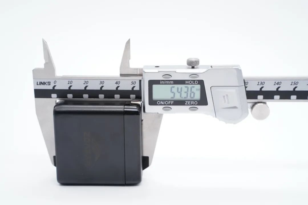
The height of the charger body is measured to be 54.36mm.

The width is 54.11mm.

The thickness is 30.14mm.

Compared with Apple's 61W charger, obviously smalle.

The intuitive feeling of holding it in your hand, it is small and exquisite.

The net weight is about 140g.

When the power is turned on, the LED indicator lights up blue.

Using ChargerLAB POWER-Z KT002 , the USB-C1 port supports Apple 2.4A, Samsung 5V2A, DCP protocol, and QC2.0/3.0, AFC, FCP, SCP, PE2.0, PD3.0, PPS fast charge protocol, Compatibility is very good.

In addition, the PDO message shows that the C1 port also has five sets of fixed voltage gears of 5V3A, 9V3A, 12V3A, 15V3A, and 20V3.25A, and a set of PPS voltage gears of 3.3-11V5A.

In addition, it is measured that the compatible protocol of the C2 port is exactly the same as that of the C1 port.

And with 5V3A, 9V3A, 12V2.5A, 15V2A, 20V1.5A five sets of fixed voltage gears, and 3.3-11V3A set of PPS voltage gears.

Use KT002 to test that the A port supports QC2.0/3.0, AFC, FCP, SCP, PE2.0 fast charge protocol.
2. Disassembly of ZONSAN 65W Gallium Nitride Charge

Disassemble the shell and take out the charger module.

The front and back of the module are covered with thermal pads and brass heat sinks, etc., and the heat sinks are soldered and fixed.
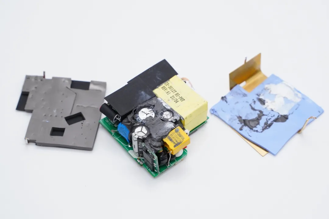
The space between the components on the front of the main board is also filled with thermally conductive glue, and the output terminal is pasted with an insulating isolation board.

The measured module length is 49.28mm.

The width is 50.12mm.

The thickness is 20.18mm.

The front of the main board is at a glance. After the silicone is cleaned, you can see that there are filter capacitors and I-shaped inductors in the center area. There is a JOULWATT JW7726B synchronous rectifier controller in the lower left corner.

At a glance on the back of the PCB board, there are JOULWATT switching power supply main control chip JW1515H, and GAN MOSFET.
It is found through observation that this charger adopts a high-frequency QR switching power supply architecture with two DC-DC secondary step-down circuits on the secondary side, and the power is intelligently distributed by the MCU. Below we start from the input terminal to understand the information of each device.

The switching power supply main control chip uses JW1515H , which is a highly integrated quasi-resonant flyback controller that supports 700V high voltage startup, integrated X capacitor discharge function, supports 8~90V wide range power supply, and does not require external voltage regulator components. Built-in high-reliability GaN direct drive circuit, 6V drive voltage can directly drive GaN devices, effectively simplifying the drive circuit design and higher reliability. Compared with competing products, the peripheral circuit of Jiehuat 1515H can save 10+ devices, effectively reducing the cost and area, and increasing the degree of freedom of layout.
As one of the leading power management IC suppliers, JOULWATT provides the industry's most comprehensive set of solutions in the field of high-power fast charging, including PFC, ACF, ZVS, QR controllers, and gallium nitride sealing , Protocol and synchronous rectifier controller, etc., the power range covers 20W~200W. JOULWATT power management IC has been widely used in domestic TOP mobile phones, notebook computers, and other brands.

JOULWATT JW1515H’s specification.

The JW7726B high-frequency synchronous rectifier controller is also from JOULWATT, supports CCM, DCM, QR and ACF modes, supports high-side and low-side applications, and has low quiescent current. During the ringing period, it can effectively prevent the synchronous rectification MOSFET from turning on by mistake; it has a fast turn-off capability to be compatible with CCM; it can effectively prevent the gate from being coupled to the turn-on voltage during the startup process (before VCC is established). It is understood that the current cumulative shipment volume of JW7726 series products is close to 10 million units .


The input terminals, the safety X capacitors are welded with long solder feet to save space, and there is a small rectifier bridge board on the left.

The patch fuse is on the back of the motherboard, with a rated current of 3.5A.

The NTC surge suppression resistor is used to suppress the power-on surge current.

The two-stage design of common mode inductor is used to filter out EMI interference.

The other close-up is also insulated with an insulating tube.

A close-up of the safety X capacitor with a capacity of 0.22μF.
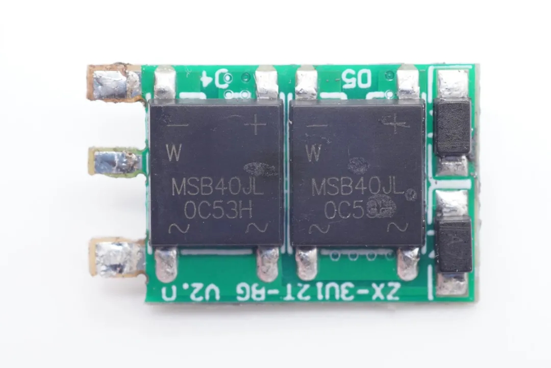
There are two MSB40JL rectifier bridges on the small board to share the heat equally.

There are no components on the back of the small board.

The side of the module, there are I-shaped inductance, high-voltage filter electrolytic capacitors, and Y capacitors in the middle.

I-shaped inductance close-up.
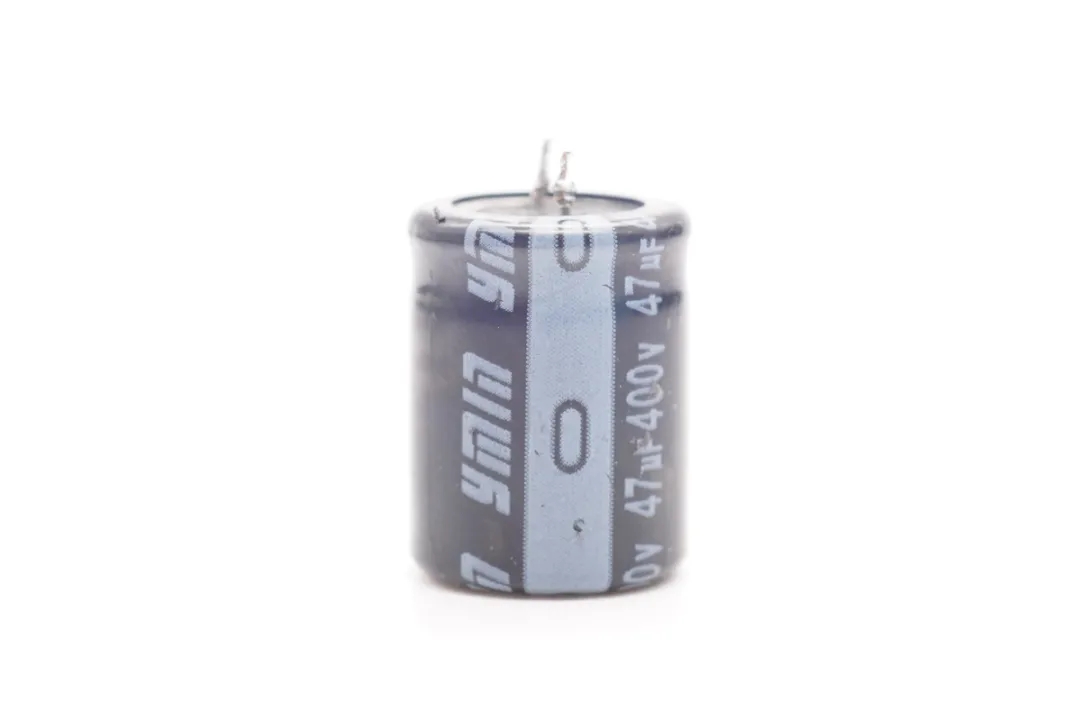
The high-voltage filter electrolytic capacitor adopts Yongming KCX series with a specification of 400V 47μF. This series of products have an operating temperature range of -55°C~105°C, a life span of 3000 hours, and have the performance advantages of lightning resistance, low leakage current (low standby power consumption), high ripple current, high frequency and low impedance.

The other two are CyXincon brand with specifications of 400V 33μF and 400V 22μF respectively.

The power supply capacitor specification of the main control chip is 50V 22μF.

he high-voltage switching MOSFET uses Innoscience INN650D02 gallium nitride power chip, with a rated withstand voltage of 650V, a peak withstand voltage of 750V, and a conduction resistance as low as 0.2Ω. It meets the industrial application requirements of the JEDEC standard, supports ESD protection, and supports Kelvin source. . The maximum working temperature is 150℃.
INN650D02 "InnoGaN" MOSFET has good high-frequency characteristics and low on-resistance, suitable for high-frequency and high-efficiency switching power supply applications. It is packaged in DFN8*8 with ultra-low thermal resistance and good heat dissipation performance. It is suitable for high-power density switching power supply applications.
It is worth mentioning that the INN650D02 "InnoGaN" MOSFET is based on the industry-leading 8-inch production and processing technology. It is currently the first mass-produced advanced gallium nitride power device on the market. The large-scale commercial use of this technology will promote nitridation. The rapid spread of gallium fast charging.

Specification of Innoscience INN650D02.

The other side is with transformer, output filter solid capacitor and indicator light. There is also a synchronous rectifier controller next to the capacitor.

A close-up of the transformer, with an information label on the top.

EL 1018 optocoupler, used for primary and secondary communication, feedback and adjust the output voltage.

The SMD Y capacitor comes from Sichuan TRX Technology Co., Ltd. It has the characteristics of small size and light weight, and is very suitable for high-density power products such as gallium nitride fast charging.
TRX focuses on the research and development, production and sales of passive components with a registered capital of 100 million yuan. There are two types of independent capacitor brands: SMD TRX and DIP TY capacitors. TRX will devote itself to the research of ceramic materials to expand the application of more categories and provide customers with more solutions.


Y capacitor close-up.

The synchronous rectifier adopts Gufeng GT52N10, withstand voltage 100V, DFN5x6 package.

A close-up of the output filter solid capacitor, the specification is 25V 1000μF.

The indicator light is close-up, and the welding foot is covered with an insulating tube.

At a glance at the output terminals, there are secondary step-down circuits on the small boards where the C1 and C2 ports are located.

Remove all the front components, and there is an MCU between the two small boards for intelligent power distribution.


The scheme adopted by the two secondary step-down circuits is exactly the same, so it can be seen that the front and back device layouts of the two small boards are the same. There are two synchronous rectifier step-down output MOS tubes and secondary filter capacitors on the front of the small board, and the capacitors are covered with insulating rubber sleeves.

The scheme adopted by the two secondary step-down circuits is exactly the same, so it can be seen that the front and back device layouts of the two small boards are the same. There are two synchronous rectifier step-down output MOS tubes and secondary filter capacitors on the front of the small board, and the capacitors are covered with insulating rubber sleeves.

The USB-C1 port step-down circuit main control chip adopts ISMARTWARE SW3516H, which is used for step-down control and protocol identification. ISMARTWARE SW3516H is a high-integrated dual-port charging chip with multiple fast charging protocols. It supports A+C port fast charging output at any port, and supports dual-port independent current limiting.
SW3516H integrates a 5A high-efficiency synchronous buck converter. Support multiple fast charging protocols such as PPS/PD/QC/AFC/FCP/SCP/PE/SFCP, maximum output PD 100W, CC/CV mode, and dual-port management logic. Only a few peripheral devices are needed to form a complete high-performance multi-fast charging protocol dual-port charging solution.


Two external R03N041AP MOS tubes output synchronous rectification and step-down.